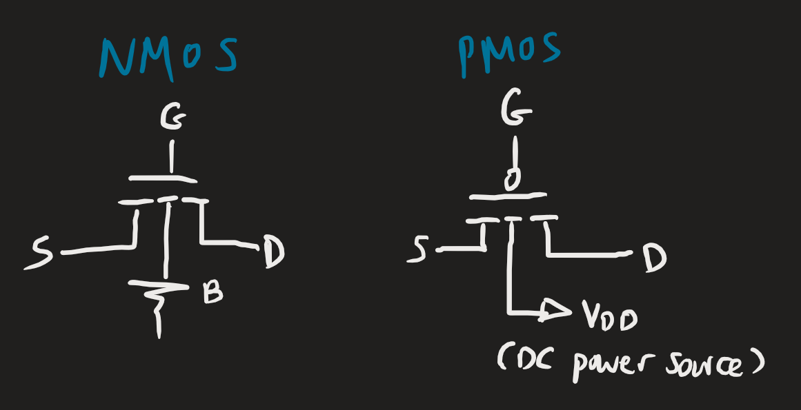
A MOSFET (metal-oxide-semiconductor field-effect transistor) is a type of transistor. There are two types of MOSFETs: PMOS transistors and NMOS transistors, fabricated with p- and n-type semiconductors, respectively.
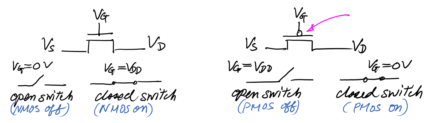 The general idea is that for the “on condition”, a conducting channel will be created between the source and drain, allowing us to conduct electricity forward.
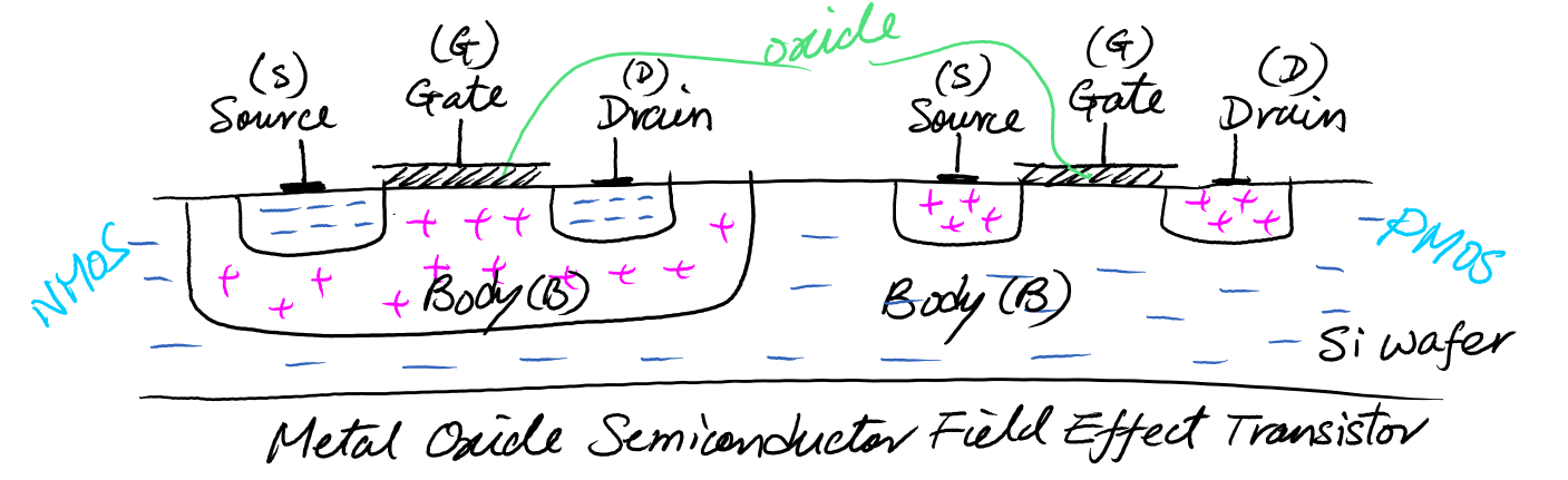
In electronic design, MOSFETs are commonly implemented in a complementary style, where we can place a PMOS and NMOS transistor on the same silicon wafer. In digital electronics, this means we have one PMOS for every NMOS transistor.
Physical structure
 MOSFETs have several key features:
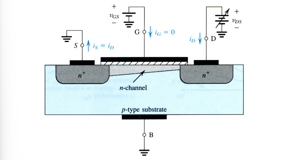
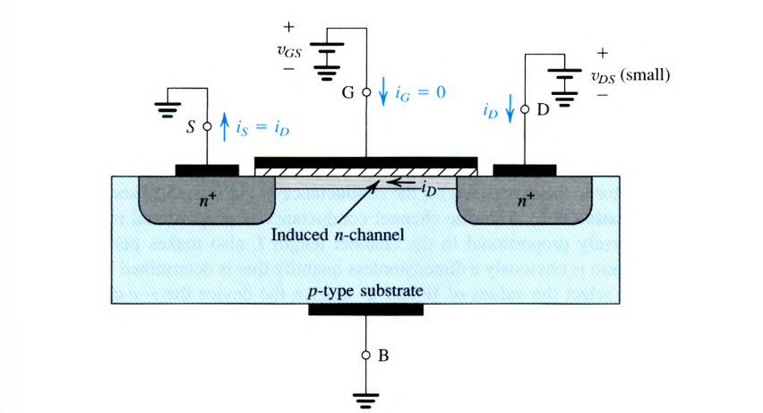
- A source (S) and drain (D) region (denoted or for NMOS and PMOS, respectively), two heavily doped regions created in the substrate.
- These can be interchanged with no change in characteristics; i.e., the device is symmetric.
- The transistor is built on a substrate, a silicon wafer that provides physical support for the device (or the entire circuit for an IC).
- Metal contacts are made to the source, drain and the substrate via the body (B).
- We assume the body has no effect on device operation. This allows us to treat the MOSFET as a three-terminal device (G, S, D).
- The body is the opposite type of the source/drain region. This means that it forms pn junctions with the source/drain regions. They’re kept in reverse-bias mode in normal operation.
- The gate electrode (G) is a terminal at the top of the device. It consists of two layers:
- An oxide layer (usually silicon dioxide) acting as an insulator with thickness is on the surface of the substrate, spanning the areas between the source and drain regions.
- A metal layer is placed on top of the oxide. Since its electrically insulated by the oxide, the current in the gate is extremely small ( A) and essentially 0 in our analysis.
- A channel region is where current will flow, from drain to source. This region has a length and width, two important parameters.
- An n-channel MOSFET is an NMOS transistor. A p-channel MOSFET is a PMOS transistor.
Induced channel
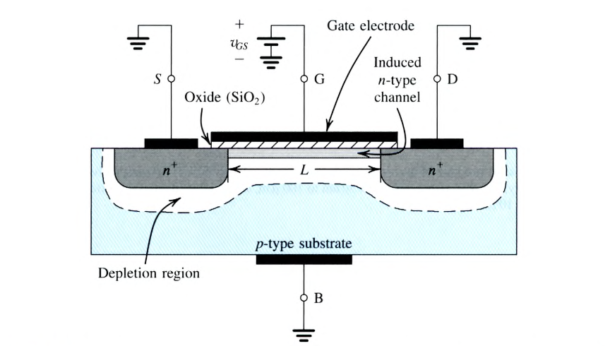
In NMOS, for the channel region to be formed. An electric field is applied at the top of the device, pushing away holes to form a depletion region. The voltage attracts electrons from the source; with enough accumulation, a region of electrons is created that connects the source and drain regions together. We form an n-channel out of a p-type wafer by inverting the substrate from p-type to n-type.
 In PMOS, for the p-channel to be formed. Note that in general the mobility of electrons is not equal to the mobility of holes, i.e., . So NMOS has better performance.
In comparison to a BJT, , and the current through the source/drain is the same.
Current and voltage equations
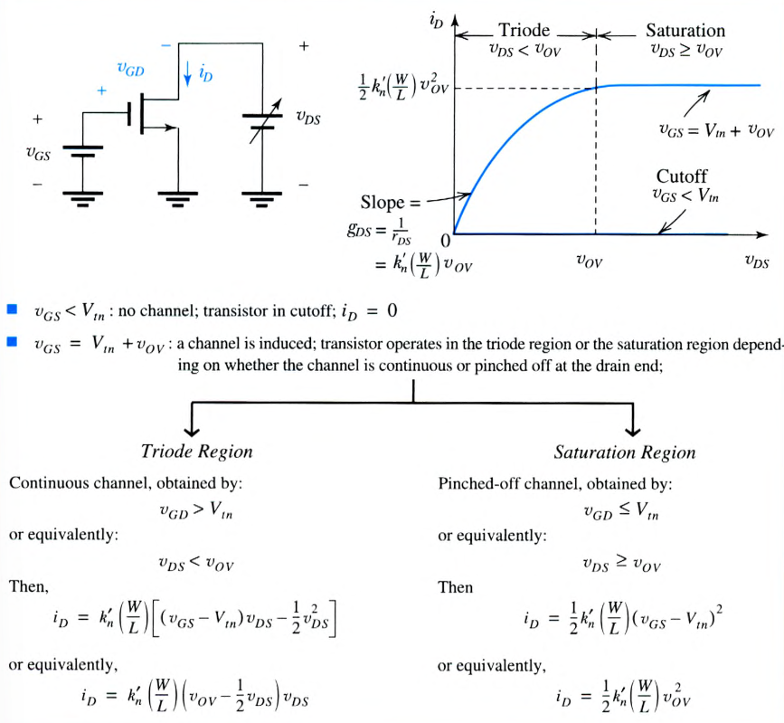
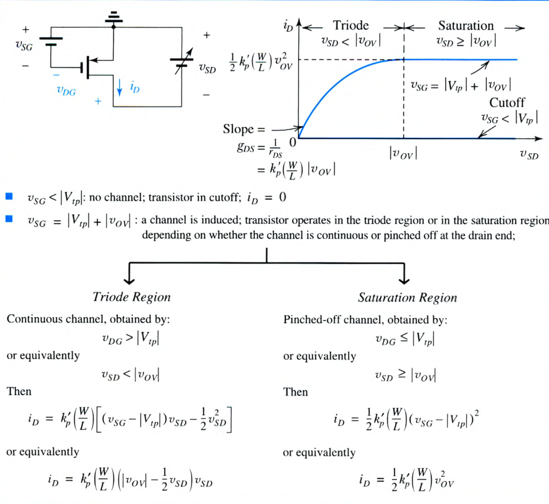
The threshold voltage () is the value of where a sufficient number of electrons accumulate to form a conducting channel, usually between 0.3 V and 1.0 V. For an NMOS, .
The overdrive voltage (; also effective voltage) determines the charge in the channel.
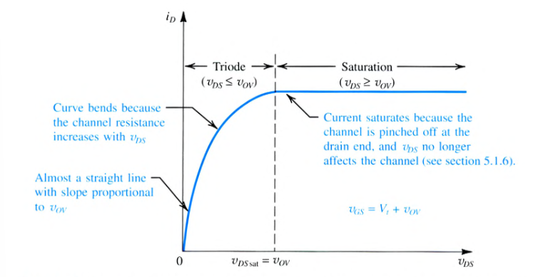
At , we have an uneven induced channel and operate in the “triode region”, which is reflected in the current formula:
 The i-v characteristic is usually measured with respect to . As we increase such that , the channel is “pinched off” and the current remains constant at the value it was at when . This current in the saturation region is given by:
i.e., is no longer dependent on in saturation mode. At the edge of triode/saturation regions, .
Parameters
The charge in the channel is given by:
The oxide capacitance is a constant, specific to the device:
The transconductance parameter () is a property of the device:
The conductance of the channel () is:
The Early voltage () is dependent on , measured in volts:
The output resistance is given by the below, where is the drain current without channel-length modulation taken into account:
Circuit analysis
For digital circuits, see the page on CMOS.
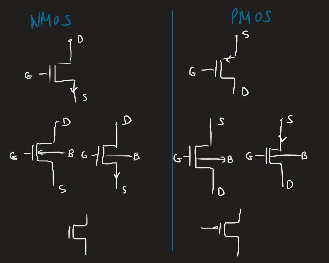
We have many circuit symbols. The arrow is always on the source terminal. If pointing out of the gate, it’s NMOS. If pointing in, it’s PMOS.
Analysis is usually done according to the mode of operation. It’s a good idea to assume we’re operating in saturation mode, since there are fewer unknowns. Some steps:
- Check if the transistor is not in cut-off mode.
- Then assume a mode of operation. Usually we start with saturation. If the question specifies at the edge, then either equation works.
- For a small signal question, assume saturation.
- Check for internal consistency with voltage inequalities. If inconsistent, then try the opposite operating region.
Note that the configuration below, the diode-connected transistor, is always in saturation.

Reference charts
Both from Sedra/Smith 8th edition.
Physics
The field-effect in the name comes from an induced electric field. The gate and channel region of the MOSFET act like a capacitor (where the oxide is the dielectric). In NMOS, positive charge accumulates at the gate, and electrons accumulate in the channel. The resulting electric field controls the amount of charge in the channel, thus the channel conductivity, thus the current that flows through the channel when is applied.
For small , our induced channel is more uniform, and behaves functionally like a linear resistance:
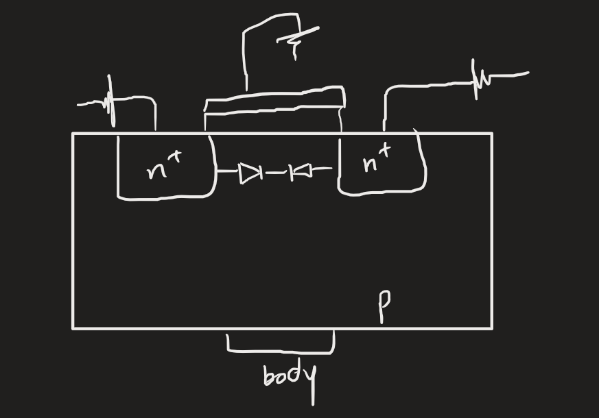
 At , we have no conduction between the drain and source. We functionally have two diodes connected opposite to each other:
The Dennard scaling law roughly associates the size of transistors with their power density.