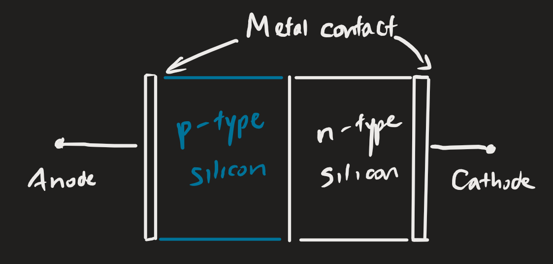
The pn junction is a type of semiconductor structure, consisting of a p-type and n-type semiconductor. They show up in many electronic devices: as the main structure of diodes, but also within MOSFETs and BJTs.
 The pn junction can conduct a substantial amount of current in the forward direction and almost no current in the reverse direction.
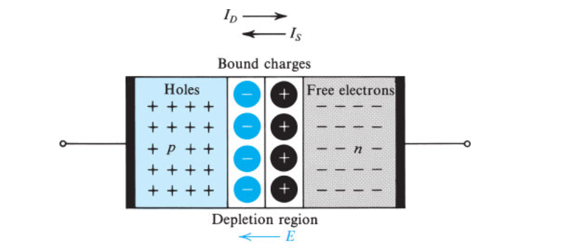
The p-type accepts some of the electrons in the n-type, causing a depletion region that blocks free electron flow. When a voltage is applied, the electron flow passes a threshold voltage barrier (barrier gets weaker with external voltage) that allows current flow (forward bias). If a negative voltage is applied, the depletion region’s size increases, preventing current flow.
Open and closed circuit conditions
Under open circuit conditions, where the junction is unconnected to any driver, there exists a depletion region. The holes are concentrated in the p-region so they diffuse across the junction to the n-side, and electrons diffuse from the n-side to the p-side.1
Addendums
In practice, both the p- and n-regions are part of the same silicon crystal, i.e., the junction is formed by creating regions of different dopings.
Footnotes
-
“A self-balancing act.” - Prof Kosteski ↩