A bipolar junction transistor (BJT) is a type of transistor; it is one of the two main types, along with the MOSFET. BJTs are used more in discrete circuits (i.e., PCBs) than in integrated circuits, due to size constraints but they still find broad use in high voltage and high frequency applications.
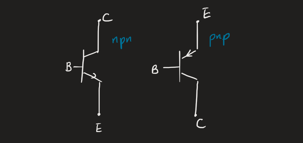
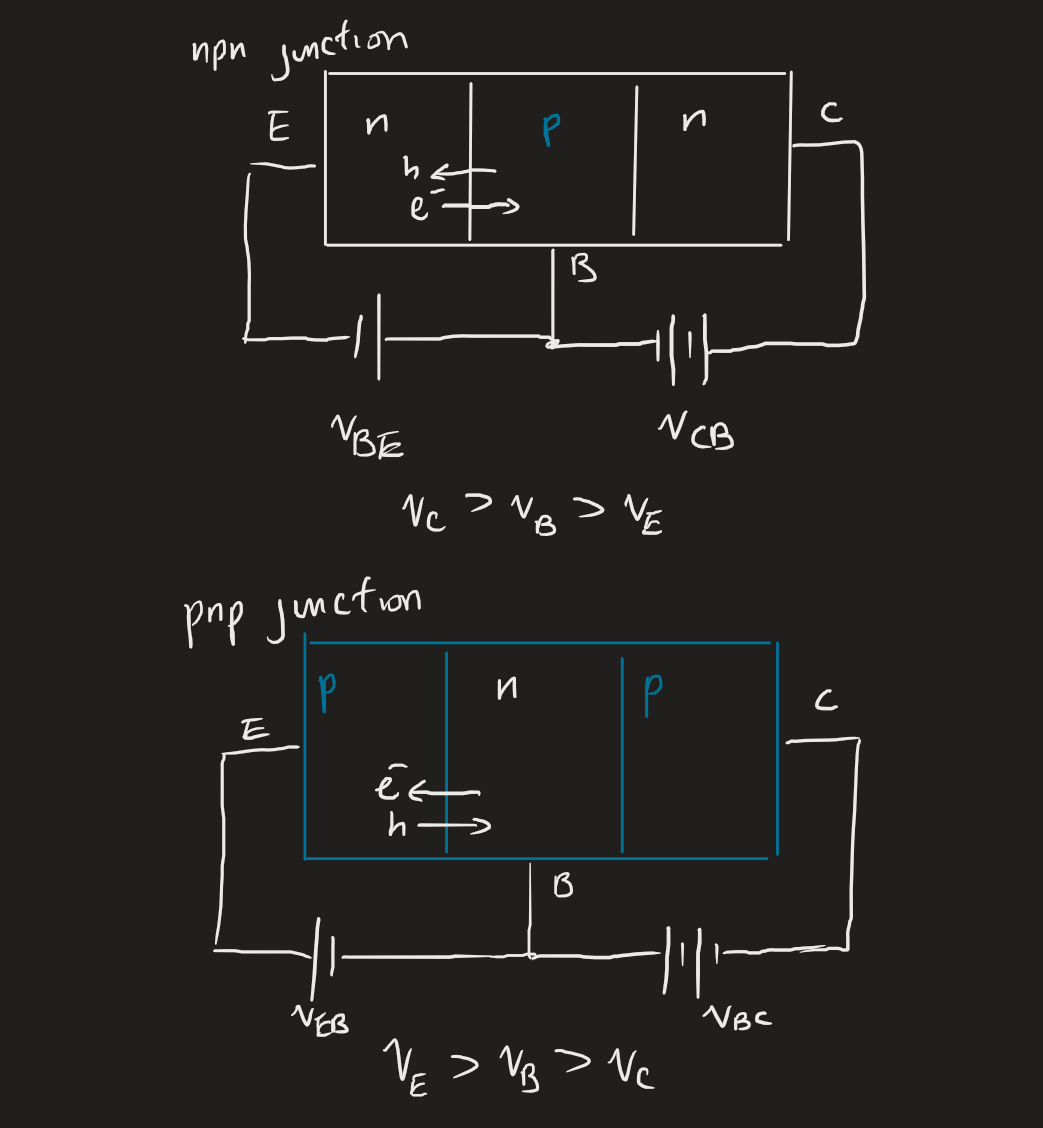
BJTs have three main terminals: the base, collector, and emitter. Depending on the internal structure, we have two types of BJTs: the npn transistor and the pnp transistor. In either case, the circuit symbol has the arrow on the emitter side, which denotes a pn junction.
Equations
Some parameters we define:
- is the common-emitter current gain, usually in the range 50 to 200.
- For a high , the base should be thin ( small) and lightly doped with the emitter being heavily doped.
- is the common-base current gain.
The collector current is given by:
The base current is given by:
The emitter current is given by:
We usually define in terms of :
Note that only the current equations are related to each other. The voltage equations are not and are still derived via Ohm’s law. Also note that compared to a MOSFET, the current through each terminal is distinct from each other, and .
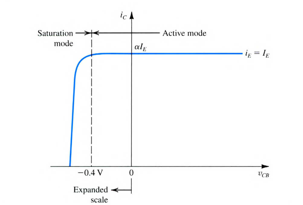
While in saturation, the ratio is lower than normally is:
Circuit analysis
We also have three modes of operation:
- At active mode, the EBJ is forward-biased and CBJ is reverse-biased.
- For an npn, we assume and .
- For a pnp, we assume and .
- At cut-off, both are at reverse-bias.
- At saturation, both are at forward bias.
The edge of saturation/active mode is at V. We say that at the edge of saturation, V. The voltage values above are standard assumptions if they don’t give us too much to work with.
As we solve for the values in a BJT circuit at DC, we assume a certain mode of operation, then check for consistency. A great tip is to draw diodes to correspond with the pn junctions. This gives an easier frame of reference for forward/reverse bias in the junctions. If we get values inconsistent with the operating mode, we chose wrong and we try again with a different mode.
Odds are that the information they give is incomplete and we can’t exactly solve with the above equations. In those cases, we must turn to KVL and take a mesh. We may also need to use Thévenin’s theorem to simplify the circuit connected to the base (which we usually don’t need to do for the MOSFET, because ).
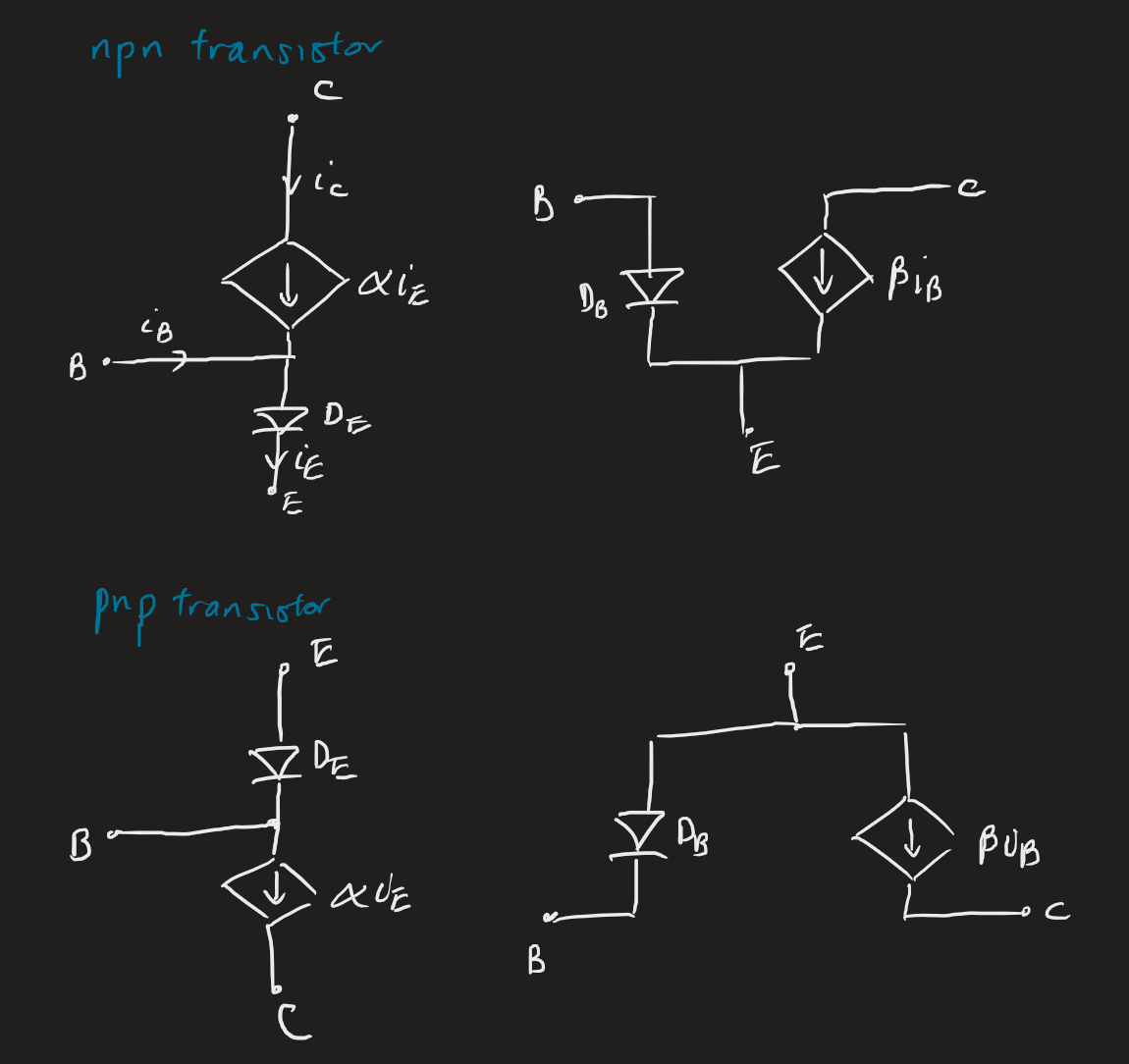
Circuit models
BJTs can be represented with equivalent circuits for any , called the large-signal models.
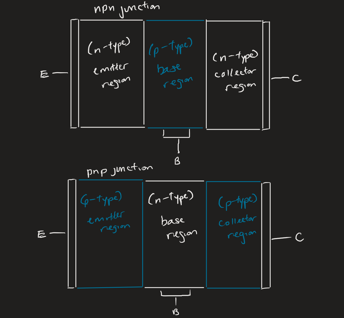
Physical structure
The two main semiconductor structures consist of two n/p-types and one of the other. Some observations at this stage:
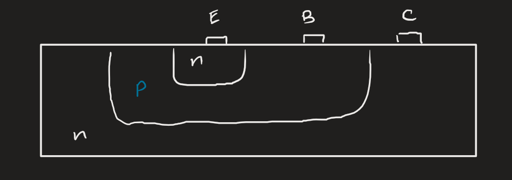
- The terminals are connected to the semiconductor via a metal contact.
- We call the transition regions the emitter-base junction (EBJ) and the collector-base junction (CBJ). The bias conditions of these regions give us the different modes of operation.
- Each region is physically connected internally. This means that the structures below are not equivalent to wiring up two discrete diodes in a circuit.
 Both electrons and holes will move when current is conducted. In the npn transistor, the emitter is the region where electrons emits from, and the collector is where electrons go. We call the movement of electrons injection. The base is where they’re in transit. Holes will undergo the opposite movement. A mirror set of movements occur in a pnp transistor.
The result is a voltage profile that looks like this:
 When BJTs are fabricated, the device isn’t symmetrical so the device has an orientation in practice. This means electrons injected into the base won’t escape being collected; is close to unity and is large. is typically much larger than , due to the larger area (and diode properties).
Addendums
Why don’t we use BJTs for digital applications? Removing BJTs from saturation can take a relatively long delay to ensure the charge stored in the base is removed.