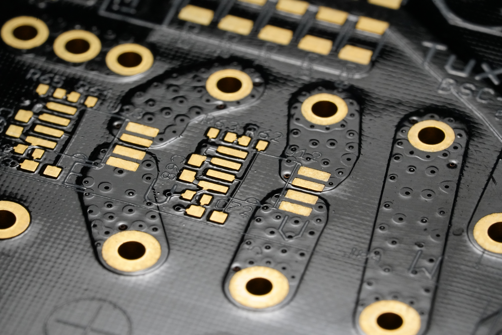
Printed circuit boards (PCBs) contain and connect electronic components, like ICs, within a compact (often layered) environment.
PCBs are designed with ECAD tools, like Altium or KiCad.
Terminology
Some important terms:1
- Trace (or track): copper connection between two components in a PCB layout.
- Layer: will include copper connections and components. PCBs have two kinds of layers: plane and signal layers. Plane layers are large uninterrupted copper regions covering the entire layer. Signal layers only have copper traces to connect PCB components.
- Laminate: insulating material used to separate copper layers.
- Stack-up (or layer stack): the arrangement of layers used to show a bare PCB.
On the production process:
- Fabrication: the first half of the manufacturing process; from a bare PCB, each layer is fabricated, and copper features are etched on.
- Assembly (PCBA): as a noun, a fully assembled PCB. Also the assembly process, where components are soldered onto a bare PCB.
Types of CAD documents:
- Schematic sheets: drawings to show component connections (like a circuit diagram).
- Bill of materials: list of all components used in the design. Used to order components and to aid assembly.
- Layout: shows the physical placement of components and connections between them. Will describe the layer stack used in the design.
- Libraries: stores CAD data for components (schematic symbols, PCB footprints, 3D models, SPICE subcircuits). May also store procurement information for each component (distributor, description, quantities, possible alternatives).
Materials
PCBs are typically made with rigid laminates. They’re there to separate the plane and signal layers (and are electrical insulators) and support the layers above and below. Using flexible materials means the layer counts tend to be much lower, but this is for when circuit boards are used in tight spaces (like cameras, smartphones).
Components
Through-hole components are soldered into via holes on the surface layer and can connect to an internal layer if necessary. Surface mount components attach directly to exposed copper pads.2
Design process
PCB design involves mechanical engineering, electrical engineering, drawing creation, writing firmware for the board, and manufacturing.
Design begins with physical constraints — maybe the enclosure has specific ports in locations we need to keep in mind. Oftentimes these mechanical constraints mean specific connectors are grouped together. When skip an enclosure? Basically never. We should especially use one if anything uses a high voltage or current or needs environmental protection. Because of these constraints Altium suggests this workflow:
- Schematic design and mechanical design are performed before PCB layout.
- Any constraints on component placement/sizes, board sizes, mounting holes are determined.
- Required board shape and mounting style is implemented.
- Components are arranged and checked against limits.
- The design is routed and layout is evaluated after components are adjusted.
Reviewing the design before manufacturing is important. Altium suggests this process:
- Final design rule check to catch any problems the automated tool didn’t catch.
- Functional review: to review whether the board performs its intended function. Last chance to adjust features or connections.
- Supply chain review, mechanical review — checking for component shortages, if the board can fit in its enclosure.
- Software and firmware review
Sub-pages
Unsorted notes
Male - header, female - receptacle/socket connectors on edges, not middle! convenient for others to interface sort connectors by use - good idea but not always necessary top layer vert, bottom layer horizontal
Footnotes
-
From Some Basic Terms. ↩
-
From Anatomy of a PCB. ↩