In PCB design, routing is the practice of making connections between components on the board.
Some components aren’t able to move — like connectors or large ICs with heat sinks. Other components can be moved. Some considerations:
- Some nets are best routed with polygons, others with traces.
- Which layers will be routed on? How many layer transitions between vias are necessary? Layer transitions should be minimised.
- Some signals can be routed as buses, while others must be routed point-to-point.
Traces may carry high current, specifically power nets and ground. In Altium, these connections are not normally routed as traces, and instead as polygons, because traces will be defined with curved ends.
Routing design
Questions to think about before traces are routed, especially considering what type of device is being made:
- Where will IO power connections be placed?
- Which components are close enough that can be quickly connected?
- Do any components share nets such that they can be quickly connected (with traces/polygons)?
- But moving components around is fine!
Altium has a few big tools. One of them is interactive routing, which is point and click. Some programs have autorouters, but this isn’t recommended in general because they can only really solve simple layouts.
There shouldn’t be any need to route back and forth across the board. In cases like this component placement should just be changed.
Impedance profiles
Single-ended traces have a characteristic impedance. Trace widths will determine the impedance. We can use the formulas below to solve for impedance/width/whatever:
For differential impedance, we usually have .
Luckily ECAD tools have calculator tools. In the stack-up, we can give a given layer an impedance profile and input a target impedance. The tool will do the geometric calculations.
Routing with traces will depend on the impedance needed:
- If it needs to be a specific value, then the width should be calculated with the thickness of the dielectric and its dielectric constant.
- If it doesn’t need to be controlled, then the trace width should be chosen to ensure easy routing and prevent design rule errors.
We want to ensure ground layers are continuous over a source and load we’re measuring. Thus, we always route traces with digital or analogue (time-varying) signals over a ground plane or large grounded polygon (DC is fine). To ensure continuity (mainly to ensure we’re measuring the right impedance), we also want to connect all ground regions used to support routing either with vias or with direct copper connections.
To apply design rules, it’s a good idea to group common traces/signals in net classes. Only traces that need targeted impedance will need an impedance rule. Groups of nets should be on the same layer, and so should differential traces.
All of the traces that make up a bus should be routed as a group ideally on the same layer. This may take up a significant amount of space in parallel bus interfaces (especially high speed ones).
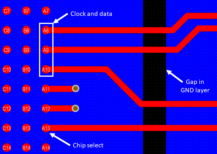
It’s also important not to route over splits in ground planes (very easy to spot), especially with high speed digital signals. Some guidelines:
- If a digital bitstream is carried through a trace, it should be routed adjacent to an unbroken ground plane.
- If a signal infrequently changes from low voltage to logic level, sometimes routing over a split is okay.
- If a DC signal, usually safe but still better.
- If high frequency, then should always be routed over an unbroken ground plane and use copper pour around the trace.