In printed circuit boards, connections between layers are made with vias. A simple type is a “through-hole via” which spans the entire stack-up. Blind vias connect a surface to internal layer, and buried vias entirely pass through internal layers.
In the ECAD tool, vias must define the drilled hole diameter and the pad/annular ring. Both are differently coloured areas. The idea is that the trace width needs to be balanced with the appropriate via size. Hole sizes should be no smaller than 8 mm (can’t be drilled).
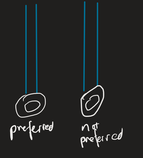
The via entry should be straight in and not at an angle.
 Three classes of annular rings are standardised:
- Class 1: throwaway products not for long-term use, no requirements
- Class 2: long-term use. Must be at least 4 mm, i.e., at least drill diameter + 8 mm
- Class 3: life-critical applications. Must be at least 5 mm, i.e., at least drill diameter + 10 mm
Via impedance usually doesn’t matter, except in high frequency or high speed designs. The most important design consideration is making the diameter small enough to place vias between traces and components.
A grounded via that runs along a signal carrying via is used to maintain signal integrity. Ideally the distance should be as close to the layer thickness as possible to ensure the greatest noise suppression, especially in high-speed signals. Otherwise we’d get quite a bit of electromagnetic interference.