In printed circuit boards, traces (or tracks) are copper connections between two components in a layout. Traces carry signals, some of which might require a specific impedance (usually ).
The design choice of which trace width to use will depend on three goals:
- Hitting an impedance target
- Ensuring you can carry enough current1
- Trace density, i.e., traces will be densely packed so a thinner trace would make room for all connections
The value will also depend on the fabricator’s limitations. A good lower bound is around 5 mm, preferably 8-10 mm, and upper bound around 20 mm. These can be specified as design rules.
Signalling
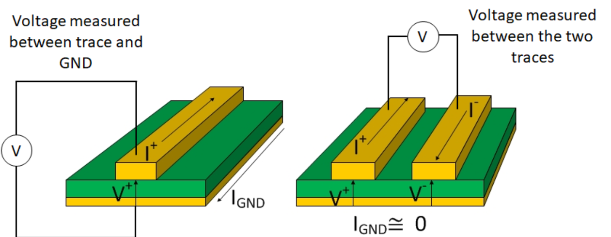
There are two main types of signalling: single-ended signals and differential signals. Differential pairs are most used in high-speed design (including computer interfacing, like USB, Ethernet, [HDMI]). Nevertheless this isn’t a firm rule.
 In Altium, traces in a differential pair will be suffixed in
 _P and _N for the positive/negative terminals, respectively. They should be kept at a specific distance apart, which should be maintained. And as with single-ended traces, it’s preferable to route short, direct routes.
Differential pairs should have close to the same length to ensure noise is the same and signals are read properly. Sometimes it’s not possible so some small curves are needed to match the length. To do so, we can apply a “length matching tool” (in the toolbar)
Types
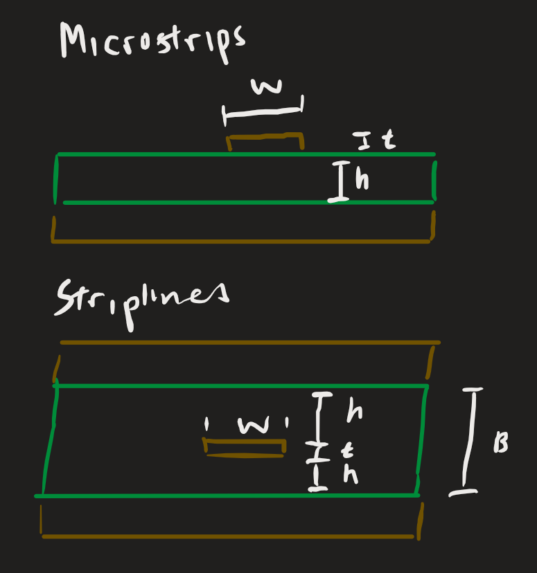
The two most common trace designs are microstrips and striplines. Microstrips are routed on surface layers and striplines are routed on internal layers.
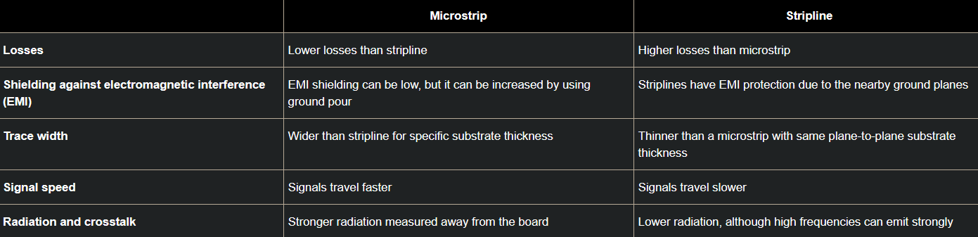
 Which style to use? Up to the designer. This table is a good reference:2
 There’s freedom to choose as long as an appropriate layer is dedicated to routing the signals. Some components (like large processors) will require stripline routing and microstrip routing because of how many pins there are.
Footnotes
-
TL;DR see resistivity for resulting resistance that may cause power loss. ↩
-
From Microstrips vs. Striplines. ↩