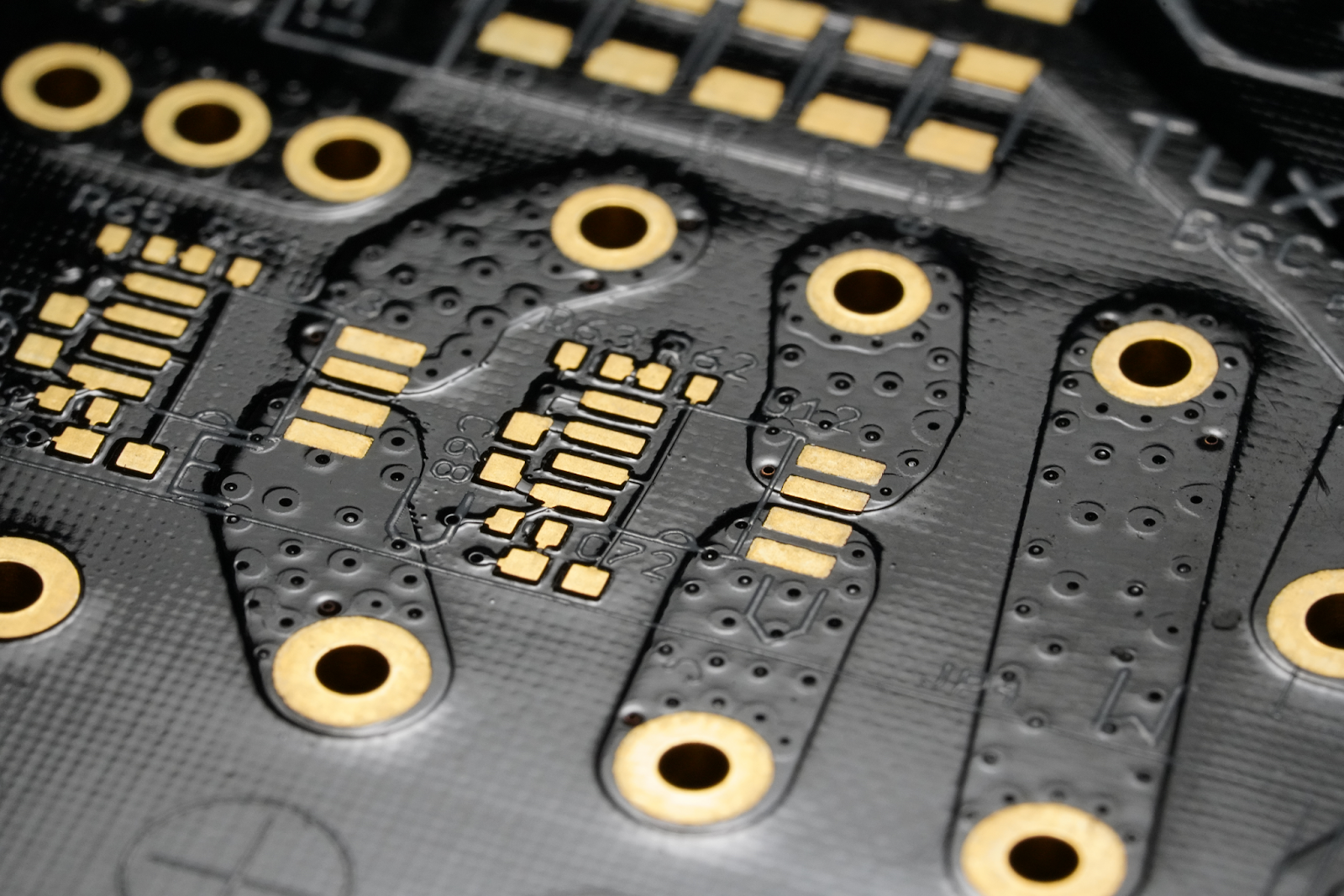
In PCB design, a schematic sheet is a drawing that shows important connections between components, power, ground, and other explanatory notes that are necessary to show how the design works. Design projects could have several schematic sheets, with important pieces of information that may not be in the PCB layout.
Anatomy
In schematic sheets, we have:
- All components used in the design.
- Nets that electrically connect components.
- Any components that may be part of an interconnect.
- Power and ground connections.
- Port connections used to define nets that span multiple sheets.
We don’t have:
- The IRL physical location of components.
- What the nets are composed of.
- What the interconnects pass through.
- What is used to supply power to components.
- How copper is routed between ports.
Since there will be multiple schematics in a project, we shouldn’t put every single circuit into the same schematic sheet. In particular, some components may have a large number of pins, so they’re difficult to represent in one block diagram. In this case, we use multiple diagrams for the same component (with only a single footprint).
Important information is in the bottom-right. The “number” is like a page number.

We can connect different schematic sheets with ports and harnesses. A port denotes a single connection between two sheets. Harnesses connect multiple ports.
Types
There are two main types of schematics used in PCB design — flat schematics and hierarchical schematics. Hierarchical schematics have a top-level sheet and multiple sub-sheets (with IO). Being top-level allows it to easily repeat groups of circuits. Flat schematics don’t have an enforced hierarchy, i.e., they’re just a collection of schematic sheets.
Design
When thinking about design, some good initial questions are:
- Do we know which types of circuits we need in each section of the PCB?
- Will the circuits need to be repeated in multiple places?
- What power sources do we need (i.e., multiple voltage levels)?
- Will there be more than one ground net?
It’s also difficult to pick which components to use, because there are millions on the market — but there are about 20 categories of components so we can narrow things down. We can use the Manufacturer Part Search panel in Altium (bottom right, Panels). Remember to use in-stock components.
In terms of general principles, it’s a good idea to:
- Go from left to right — inputs in the left side, connect flowing to the right
- Group components that are part of the same circuit into separate areas.
- Try to avoid crossing wires — to avoid unintended connections.
- Use net names and ports instead of crossing wires.
- Use built-in power and ground symbols.
- Don’t be afraid to use multiple sheets.
- For large ICs, it’s a good idea to use net names and ports.