One major application of transistors (MOSFETs, BJTs) is as an amplifier of signals. The idea is that the transistor is operating in an active region — for MOSFETs, this is the saturation region; for BJTs, this is the active region.
Small-signal analysis is an important tool for analysing transistor amplifiers, because we can achieve almost linear amplification with an input small-signal.
Small-signal amplification
We can get close to a linear gain, if we pick a bias point to operate at. The (small-)signal we want amplified is superimposed on top, such that:
This gives us a larger .
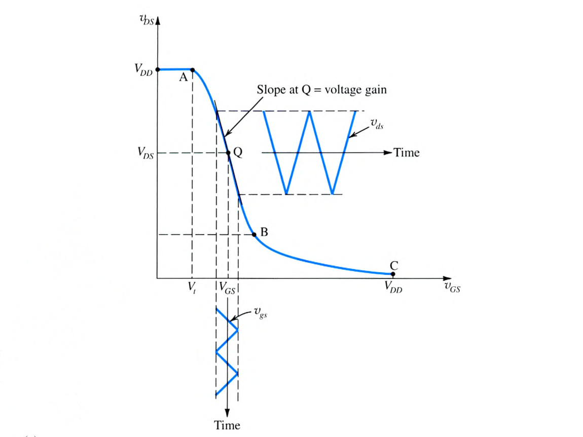 The gain is found by the tangent line to the voltage transfer characteristic, where is evaluated at the DC operating point:
For a MOSFET, the gain is given by:
i.e., the gain is negative (so we have an inverting amplifier). For a BJT, the equation is given by:
Again, the gain is inverting. Note that for both cases, the gain isn’t necessarily inverting if we don’t directly discuss the transistor inputs/outputs (which can happen in some questions).
Basic configurations
With the small signal understanding out of the way, we have three key categories of FET/BJT amplifier configurations.1
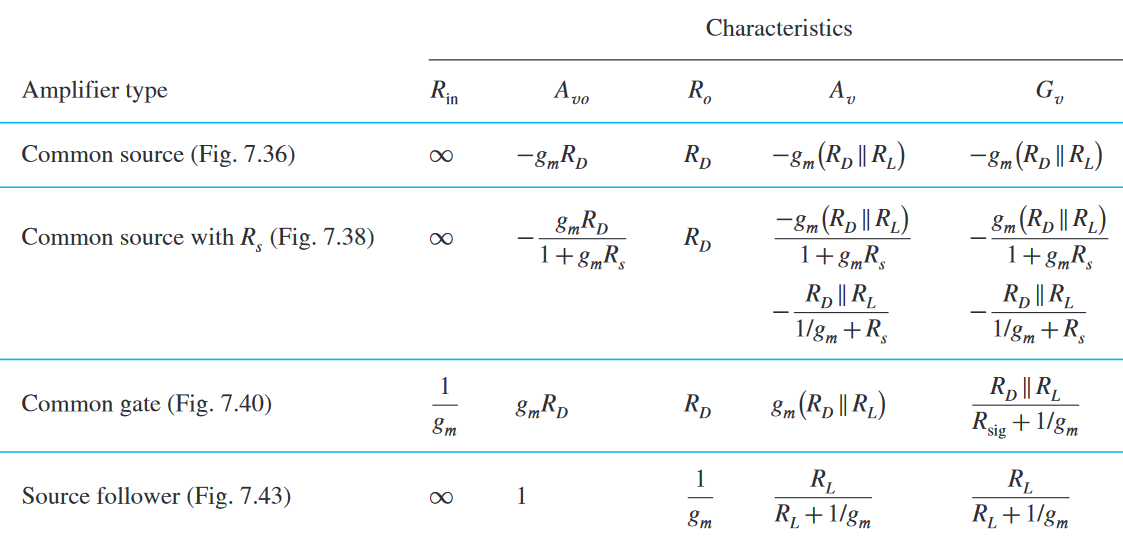
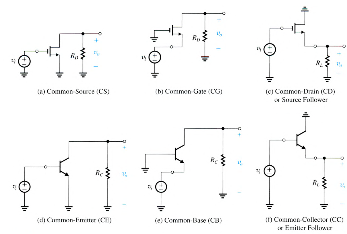 MOSFET amplifiers have the following characteristics:
 BJT amplifiers have the following characteristics:
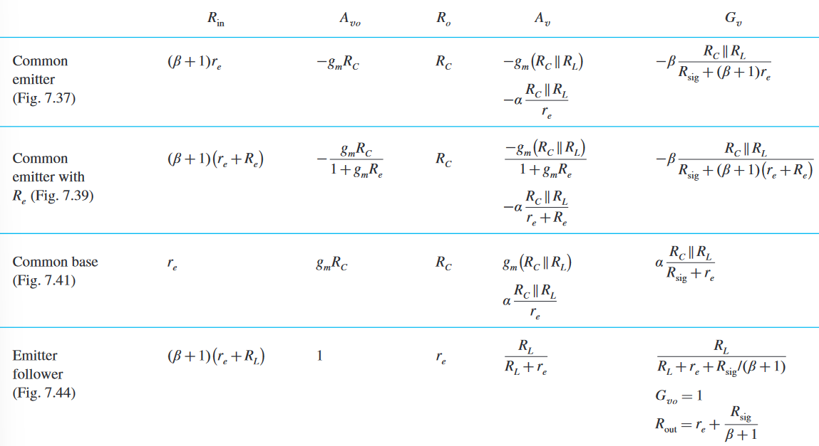 These characteristics can be derived from analysis of the small-signal models of the amplifiers. Both tables neglect the effect of due to the Early effect.
In general, when we analyse the basic configurations (as in the images above), we use the hybrid-π model. When we look into effects at the source, we use the T-model. This is mainly because there’s more to calculate with the hybrid-π model.
In the BJT case, we observe that:
This is the resistance-reflection rule, which states that the total input resistance looking into the base is times the total resistance in the emitter. This gives us more control of .
CS/CE amplifiers
The most popular MOSFET amplifier type is the common-source amplifier. Both the CS/CE amplifiers are most useful, since they have a high voltage gain and exhibit a moderate-to-high input/output resistance. They fail in their high-frequency response.
Sometimes it’s useful to add an extra source/emitter resistance / in a CS/CE amplifier. is a source-degeneration resistance because it results in some negative feedback — this improves performance (bandwidth, linearity) at the expense of some voltage gain by . We call the emitter degeneration resistance (similar to the MOSFET case) due to its negative feedback.
CD/CC amplifiers
The common-drain amplifier is also called the source follower; the common-collector amplifier is also called the emitter follower. Both have an amplifier gain of . We use follower circuits in designing small-signal amplifiers and amplifiers that handle large signals and deliver large amounts of power to a load. These function as a buffer amplifier.
The gain function for each transistor amplifier is given by:
As , , with no phase shift.
Complicated configurations
In general, when do we include the output resistance due to the Early effect? In discrete-circuit design, the resistances are usually much smaller than . In IC amplifiers, it must be included in analysis.
Note that in general, we use a voltage divider to specify the gate/base voltage. Large resistor values (in the megaohm range) are used to present a high input impedance (which is desirable). We also usually use a capacitor in between the input small-signal and the circuit to isolate from the DC analysis (otherwise we’d have an extra resistor in parallel in our divider). All of this allows us to carry out our DC bias design without the small signal component affecting the circuit results.
Footnotes
-
Images from Microelectronic Circuits, by Sedra/Smith. ↩