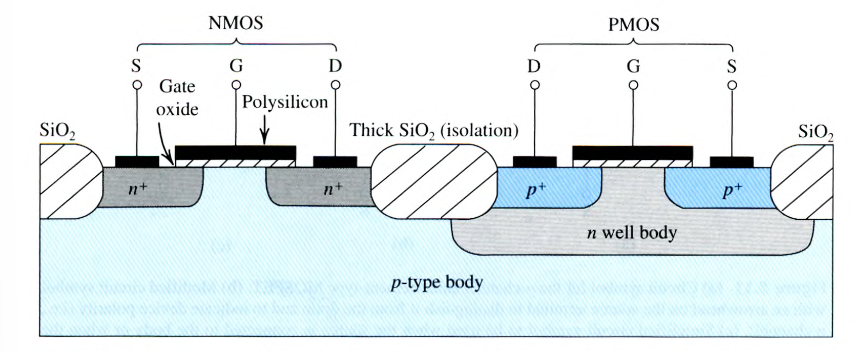
CMOS (complementary metal-oxide-semiconductor) is a design choice in MOSFET fabrication that pairs together p-type (PMOS) and n-type (NMOS) MOSFETs on the same silicon wafer, isolated by an oxide. It’s standard to have the same number of p- and n-type transistors in digital electronics design.
 In digital circuits, the general structure looks like the below:
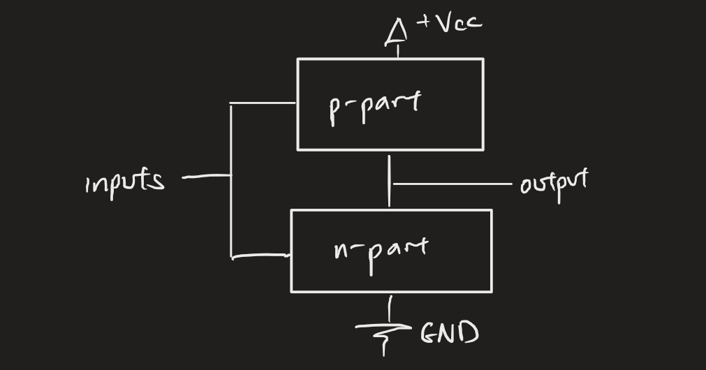 The p-part is called the pull up network, and the n-part is called the pull down network. We usually have them be on the top and bottom of the circuit, respectively (connected to VCC and ground). Stick to this.
Functions and gates
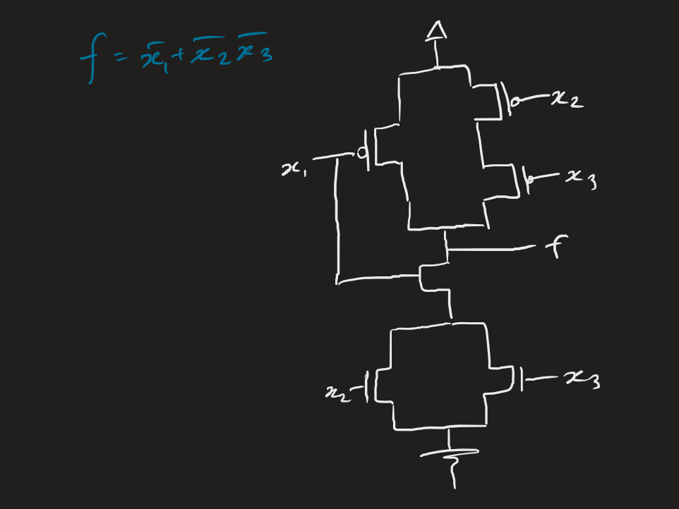
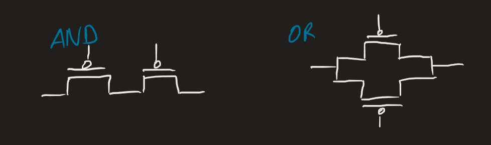 If we have a series configuration in the p-part, we have a parallel configuration in the n-part. The opposite holds true: for parallel in the p-part, we have series in the n-part.
Addendums
What if we do this the reverse way? With PMOS pulling down and NMOS pulling up? This doesn’t really work because of the transistor’s threshold voltage — we get weak ones or weak zeroes. So we don’t use NMOS to produce a logic 1 and don’t use PMOS to produce a logic zero.
One of the key benefits of CMOS technology is that they have fairly low power consumption — only when the transistor switches states will it draw power, since one set of transistors will be off. So if there are fast switches, power consumption will increase (and of course transistors leak electrons). If we used resistors to set-up logic functions instead, we’d draw an enormous amount of power, which matters more as we scale up systems.
Resources
- Design of Analog CMOS Integrated Circuits, by Behzad Razavi