The DE1-SoC is a hardware design platform from Terasic built around an Altera Cyclone V system-on-chip FPGA. It supports a hard core ARM Cortex-A9, and a soft core Nios II, by default.
We can program the board with HDLs, like Verilog, SystemVerilog, and VHDL; or alternatively with higher-level languages like Assembly languages (ARM, Nios II) or C.
FPGA
The FPGA is an Altera Cyclone V, built in 28 nm technology. It operates with a 50 GHz clock with about 85k 4-LUTs. It contains hundreds of M10K memory blocks, hundreds of RAM blocks each with 10k bits. They’re configurable in their aspect-ratio (i.e., number of rows vs. word width).
It also has built-in gated D-latches, and Quartus Prime will map any Verilog descriptions to those latches. We don’t need to worry about whether they’ll end up using NANDs or NORs.
Hardware
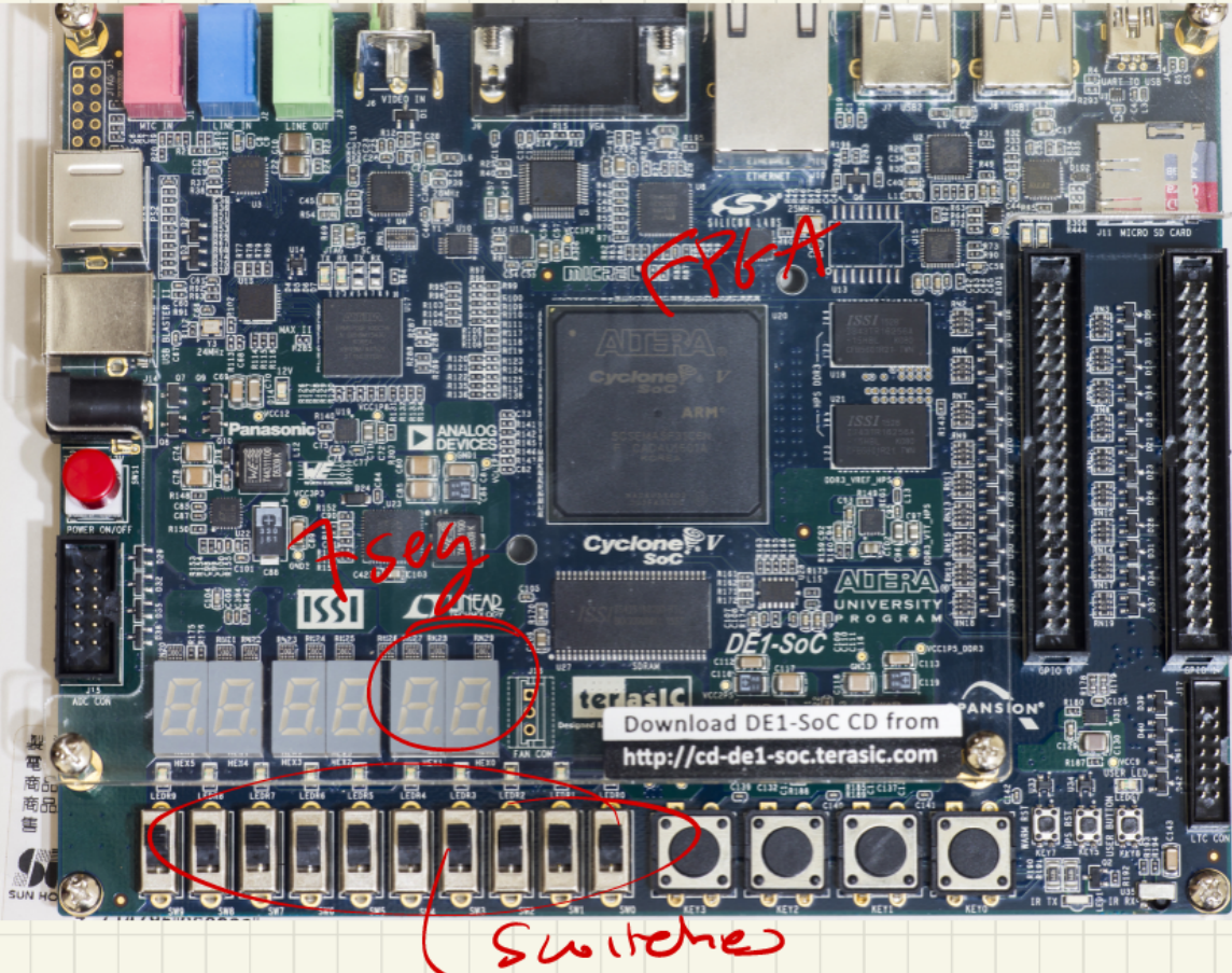
The board has seven-segment displays, toggleable switches, and LEDs. Some useful mapping:
LED[9:0]for the LEDs, mapped to address0xFF200000.SW[9:0]for the switches.HEX0[6:0]for the seven-segment display, which is a common anode. We can go up toHEX5.
Some other hardware components include:
- 2 ports for mice and keyboard
- Two GPIO parallel ports
- USB-B plug for programming the board
- ADC, at a sampling rate of 8 kHz
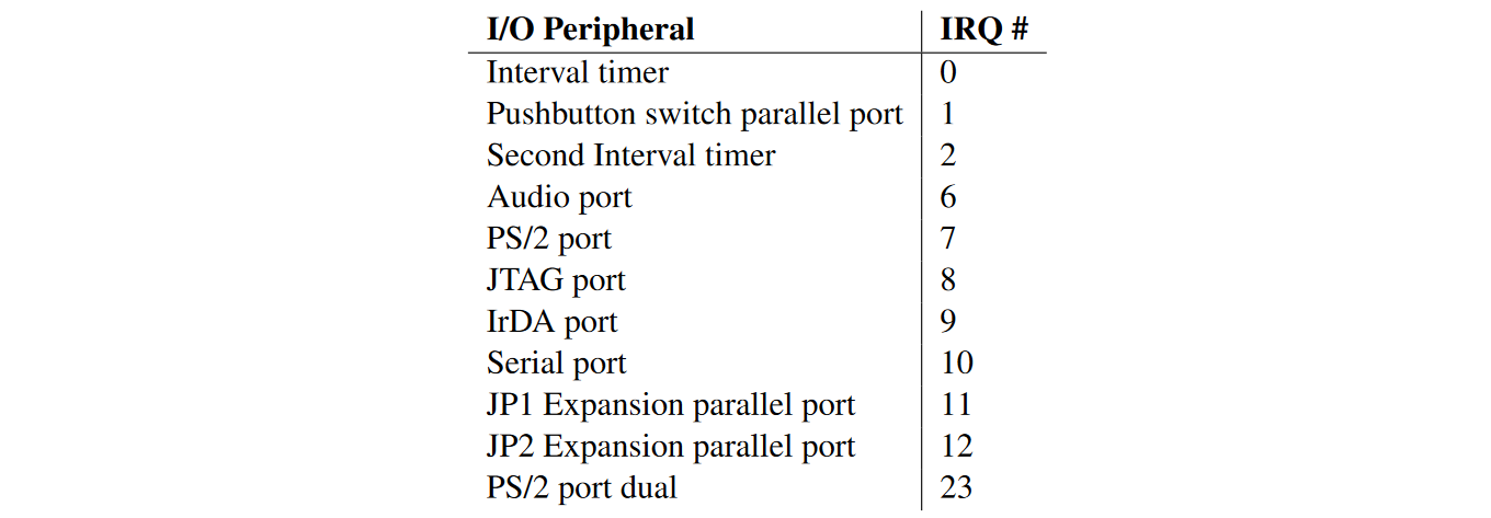
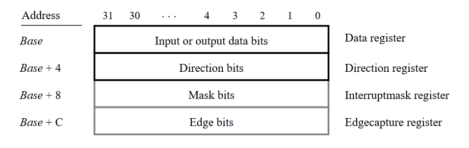
The hardware components have the following parallel port structure. At a high level, the data register gives us the current state of the device. The interrupt mask allows us to specify which bit of the device should trigger interrupts, and the edge register specifies whether the corresponding data bits have changed at any point. The edge register bits need to be reset by writing a 1 into whatever bit is currently active.
Buttons
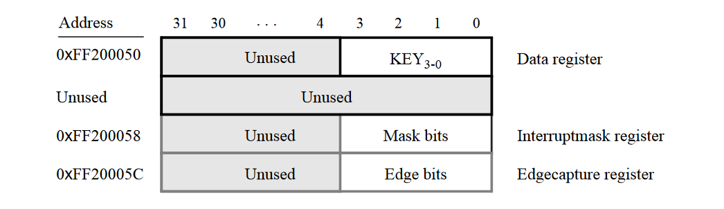
In Verilog, we use KEY[3:0] for the pressable buttons to the right of the switches. They’re mapped to address 0xFF200050. The mask register will enable interrupts from the corresponding button.
If any interrupts occur, we need to write to the edge register to de-assert the interrupt signal. The easiest way to do this by writing to the edge register its current value.
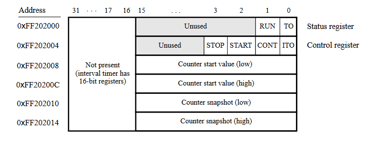
Timer
The board has two timer devices operating at a frequency of 100 MHz, with a common parallel interface design at addresses 0xFF202000 and 0xFF202020.
 An easy way to specify the high and low bits of a constant is to use:
.equ CONST 0x500000 # define some arbitrary constant
addi r12, r0, %lo(CONST) # stores lower bits in r12
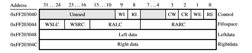
addi r13, r0, %hi(CONST) # stores higher bits in r13Audio
There are three physical ports: mic in (pink), line in (blue), line out (green).
Within the control register:
CWwill clear both output FIFOs if 1 is written to it. To resume, we write 0 into it.CRwill clear both input FIFOs. Same deal as the above.WE/REare interrupt enable bits for output/input.WI/RIare interrupt indicators.- The board will throw an interrupt when the output FIFO is less than 25% full. The idea is that we want the CPU to fill in the output FIFO so that it never runs out of signals.
Within the fifospace register:
RARC/RALC(read audio right/left channel), 8-bit numbers that tell us how many of the 128 entries of the input FIFOs are currently filled.WSRC/WSLC(write audio right/left channel), 8-bit numbers that tell us how many of the 128 entries of the output FIFOs are currently empty.
The data registers specify the left and right channels. When we write to the registers, we enqueue the output FIFO. When we read, we dequeue from the input FIFO. In software, this is an abstraction of the behaviour below the hood.
Video display
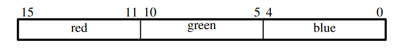
The DE1-SoC has a VGA display. Each pixel is made up of 16 bits, which express how much RGB is in the pixel. The below is how each colour is described in the frame buffer.
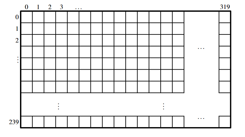
 The VGA port supports a screen resolution of , so the frame buffer has a two-dimensional coordinate system. The base address is at
 0x08000000; to access any subsequent pixels we need to change the value of y and x in our code. To write to a pixel address, we can do:
int x, y;
volatile short int *pixel_address;
pixel_address = base + (y << 10) + (x << 1);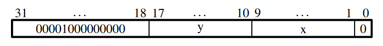
Miscellaneous
Nios II supports interrupts.